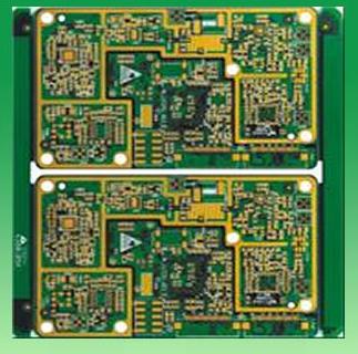
All PCB surface finished reference
PCB surface treatment is the most basic purpose is to ensure good welding or electrical properties. Due to the nature of the copper in the air tend to exist in the form of oxide, it is unlikely to remain as the original copper, so the need for other processing of copper.
1 hot air leveling (HASL)
Hot air leveling, also known as hot air solder leveling (commonly known as spray tin), it is in PCB was coated on the surface of molten tin (PB) solder and heating compressed air whole (blowing) process, which leads to the formation of a layer of both anti copper oxide, and can provide good solderability of coating layer. Copper and tin intermetallic compound formed by hot air in the combination of solder and copper. PCB hot air leveling to sink in the molten solder; air knife in the solidification of the solder before blowing flat liquid solder; air knife to the surface copper solder meniscus shape to minimize and prevent solder bridging.
2 organic and protective agent (OSP)
OSP is a printed circuit board (PCB) with a process of RoHS instructions copper surface treatment. OSP is the abbreviation of Solderability Preservatives Organic, translated as organic film, also known as copper protection agent, in English, also known as Preflux. Simply put, OSP is on the surface of cleaning bare copper, chemically grown a layer of organic film. This layer of film has oxidation resistance, thermal shock resistance, moisture resistance, is used for protecting the surface of copper in the normal environment no longer continue to rust (oxide or sulfide, etc.); but in the subsequent welding heat, this protective film must be easily flux are rapidly cleared, so can the exposed clean copper surface can be in a very short period of time and the molten solder immediately with a solid solder joint.
3 full plate nickel plated gold
Nickel plated gold on the whole plate is plated with a layer of gold on the first layer of nickel plated on the surface of PCB. The main is to prevent the diffusion of gold and copper. Now the nickel plating gold has two kinds: plating soft gold (gold, gold surface does not look bright and hard gold plating (surface smooth and hard, wear-resistant, containing cobalt and other elements, the gold surface looks brighter. Soft gold is mainly used for chip packaging when playing gold; hard gold is mainly used in welding electrical interconnection at non.
4 heavy gold
Gold is wrapped in a thick layer of copper on the surface of a thick, good electrical nickel alloy, which can protect the long-term PCB; in addition, it also has other surface treatment process does not have the tolerance of the environment. In addition, gold also can prevent the dissolution of copper, which will be beneficial to lead free assembly.
5 heavy tin
Since all of the solder is based on tin, the tin layer can match any type of solder. Shen tin process can form flat copper tin intermetallic compounds. This feature makes Shen tin with hot air leveling as well can be welding without hot air leveling headache the flatness problem; Shen tin plate can not be stored for too long, the assembly must be carried out according to the sequence of the immersion tin.
6 heavy silver
Heavy silver process between organic coating and electroless nickel / gold deposit, process is relatively simple, fast; even when exposed to heat, humidity and pollution of the environment, silver can still maintain good solderability, but will lose luster. Heavy silver does not have the good physical strength of electroless nickel / gold deposition because there is no nickel under the silver layer.
7 ENEPIG
Chemical nickel palladium and gold precipitation compared between the nickel and gold more a layer of palladium, palladium can prevent the occurrence of corrosion caused by replacement reaction, heavy gold ready to fully prepared. Gold is closely covered on the top of the palladium, providing a good contact surface.
8 hard gold plating
In order to improve the wear resistance of the product, increase the number of plug and play hard gold plating.
